Vision camera for PCB inspection and tiny defect misses
Publication Date
author
In high-mix electronics manufacturing, a vision camera for PCB inspection can determine whether tiny defect misses become costly field failures or controlled quality events. For QA and safety teams, the real challenge is not image capture alone, but measurable detection accuracy, repeatability, and noise resistance under production conditions. This article examines what truly affects defect visibility and how data-driven inspection standards reduce risk.
Why tiny defects are still missed even with a modern vision camera for PCB inspection

The core search intent behind “vision camera for PCB inspection” is usually practical, not academic. Quality managers and safety stakeholders want to know why a system that looks technically capable still misses fine scratches, micro-cracks, solder bridging, insufficient solder, lifted leads, contamination, or pad damage. They are not only looking for camera specifications. They want a reliable way to reduce escape risk on a real production line.
For most PCB applications, tiny defect misses are rarely caused by the camera alone. They usually result from a chain of factors: insufficient optical resolution, unstable illumination, poor contrast between defect and background, vibration, board positioning variation, reflective surfaces, weak inspection recipe design, and unrealistic acceptance thresholds. When these variables stack up, even a high-end system can underperform.
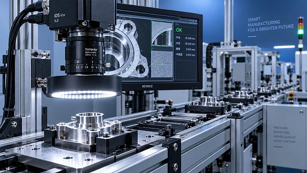
That is the first important judgment for buyers and internal evaluators: a vision camera for PCB inspection should be assessed as part of a complete inspection architecture. If the line environment, lens, lighting geometry, image processing method, and defect criteria are weak, upgrading the camera sensor alone may not improve miss rates in a meaningful way.
For QA teams, the business issue is straightforward. Every missed tiny defect can create downstream rework, customer returns, warranty claims, traceability investigations, or in safety-sensitive sectors, regulatory exposure. The inspection decision therefore has to be based on evidence: what minimum defect size is detectable, under what conditions, with what repeatability, and at what false reject rate.
What QA and safety teams actually need to verify before trusting an inspection result
Target readers in quality control and safety roles typically care about four things more than anything else. First, can the system consistently detect the defect types that matter most to field reliability? Second, how often does it miss them? Third, how stable is the result across shifts, operators, board variants, and line conditions? Fourth, what is the cost of false calls in throughput, rework, and operator burden?
That means the most useful evaluation questions are not “Is this an AI camera?” or “How many megapixels does it have?” The useful questions are more operational. What pixel coverage does the smallest critical defect receive? How sensitive is the result to board warpage or lighting drift? Can the system maintain accuracy on matte black substrates, glossy solder joints, and mixed-component assemblies? How often does the recipe need retuning after product changeover?
Safety-minded readers also want to understand defect criticality. Not every missed cosmetic issue is equal. A silkscreen imperfection may be low risk, while a solder void pattern near a power component, contamination on high-voltage spacing, or a hairline trace interruption can lead to functional failure. The inspection strategy has to rank defect modes by risk, not by visual convenience.
This is where a data-driven approach matters. Inspection systems should be qualified against a defect library tied to severity, occurrence, and detectability. If a vision camera for PCB inspection is only validated on easy samples or ideal boards, its performance claims will have limited value once production variability appears.
Camera resolution matters, but optical setup matters more than many teams expect
Resolution is often the first parameter buyers compare, but it is only one part of defect visibility. A tiny defect must occupy enough effective pixels to be distinguishable from background variation and noise. If the defect is too small relative to the field of view, no software can recover detail that the image never captured.
However, increasing sensor resolution without matching the lens, working distance, and lighting can create disappointing outcomes. A poor lens can soften edge definition. Incorrect depth of field can blur slightly warped boards. Inconsistent magnification can distort measurement. In reflective PCB environments, uncontrolled highlights can hide the very defects the additional pixels were meant to reveal.
For PCB inspection, optical design should be linked to the smallest defect class that must be reliably detected. If the critical target is a narrow solder bridge, a micro nick in a trace, or contamination near fine-pitch pads, then the system must provide enough pixel density and contrast at that exact area of interest. A broad field of view may improve throughput, but it often reduces defect detectability unless multiple inspection zones or cameras are used.
Quality teams should ask for measurable optical performance, not generic quality claims. Useful evidence includes minimum detectable defect size, modulation transfer behavior, contrast consistency across the inspection area, and repeatability on deliberately challenging samples. These indicators are more decision-relevant than headline megapixel numbers alone.
Lighting is often the hidden reason for tiny defect misses
In many PCB applications, lighting geometry determines whether a defect is visible at all. The same board can appear easy or impossible to inspect depending on whether the illumination emphasizes texture, height change, edge contrast, or reflectivity differences. This is especially true for solder joints, metallic pads, conformal coating surfaces, and contamination that only appears under specific angles.
Bright field lighting may work for some printed features but fail on low-contrast surface flaws. Dark field lighting can reveal scratches or raised contamination, but it may also exaggerate harmless texture. Coaxial lighting can help with flat reflective areas, while structured or multi-angle lighting can separate true defects from cosmetic variation. There is no single universal lighting mode for all PCB defect classes.
For high-mix production, this becomes more difficult because one line may process boards with different solder masks, finishes, component heights, and layout densities. A vision camera for PCB inspection must therefore be paired with a lighting strategy that is configurable yet stable. If each product change requires extensive manual tuning, inspection reliability may degrade over time due to setup variability.
A practical recommendation is to validate lighting against the hardest cases, not the average cases. If inspection only works when the board is clean, flat, and perfectly aligned, then the process is not robust enough for production reality. Quality leaders should demand test evidence under realistic line contamination, minor board variation, and normal environmental fluctuations.
Algorithm quality and recipe discipline decide whether captured images become trustworthy decisions
Even with good images, defect misses can remain high if the inspection logic is weak. Rule-based image processing may be effective for stable and well-defined features, but it can struggle with natural variation across suppliers, batches, and board revisions. AI-based methods can improve classification in complex scenes, yet they also introduce dependency on training data quality and edge-case coverage.
The key issue is not whether the algorithm is traditional or AI-driven. The issue is whether the inspection logic has been validated against true production variation. A model trained on clean golden samples may fail when paste volume shifts slightly, solder finish changes, or lighting ages over time. Similarly, a manually tuned threshold recipe may collapse when one supplier introduces a subtle color variation in substrate or mask.
This is why recipe governance matters. Inspection settings should be version-controlled, traceable, and tied to approved defect criteria. Changes should be documented and revalidated. Otherwise, quality drift can occur quietly, especially on high-mix lines where engineers frequently optimize for false reject reduction and inadvertently weaken true defect sensitivity.
For quality control teams, a strong supplier or internal automation team should be able to provide confusion-matrix style evidence: true positives, false negatives, false positives, and performance by defect category. Without this level of reporting, it is difficult to judge whether the system is improving risk control or simply shifting the burden to manual review.
How to evaluate a PCB inspection system without being misled by attractive demos
Many inspection solutions perform well in demonstrations because the test conditions are controlled, the boards are curated, and the defect set is limited. A more useful evaluation approach is to run a structured acceptance test using your own boards, your own known defect modes, and your own production constraints.
Start by defining critical-to-quality defect classes. Separate safety-relevant and function-relevant issues from cosmetic issues. Then identify the smallest or lowest-contrast examples in each category. These are the samples that reveal whether the system has real capability or only performs well on obvious defects.
Next, measure performance under normal production variability. Include different board finishes, line speeds, operators, and times of day if possible. Test borderline acceptable conditions as well as clear rejects. This matters because the hardest inspection decisions often happen at the boundary between acceptable and unacceptable, where inconsistent classification can damage both quality and throughput.
Also verify gage-like repeatability. If the same board is inspected multiple times, is the result stable? If it is inspected after slight repositioning, does the defect remain detectable? If the answer is no, then the process may be too fragile for quality assurance use, even if average benchmark accuracy appears strong.
Finally, review maintainability. A technically impressive system that requires constant expert intervention may not support long-term production quality. For many facilities, sustainable performance depends on whether technicians can recalibrate, verify, and troubleshoot the system without excessive downtime or specialist dependency.
Key metrics that matter more than marketing claims
For decision-makers, inspection performance should be translated into operational metrics. The most important include minimum detectable defect size for each critical defect class, false negative rate, false positive rate, repeatability across repeated runs, sensitivity to board and lighting variation, cycle time impact, and recipe changeover effort.
False negatives deserve special focus because they are directly tied to escape risk. A low false reject rate may look attractive operationally, but if it is achieved by reducing defect sensitivity, the apparent efficiency gain can be costly later. Quality teams should balance both sides of the equation rather than optimizing for one metric in isolation.
Another important metric is defect detection by severity level. A system that occasionally misses low-risk cosmetic flaws may still be acceptable, while even rare misses on critical solder or conductor defects may not be. This is why a severity-weighted validation framework is more meaningful than a single headline accuracy figure.
Traceability also matters. Can the system store images, metadata, timestamps, and pass-fail rationale for later review? For regulated or safety-conscious operations, this capability supports root-cause analysis, supplier discussions, and customer evidence. A vision camera for PCB inspection creates more value when it contributes to a traceable quality system, not just a pass-fail gate.
When a vision camera upgrade is justified and when the bottleneck is elsewhere
Upgrading the camera is justified when analysis shows that the current system lacks the required pixel density, dynamic range, frame stability, or noise performance for critical defect classes. It may also be necessary when production speed has increased beyond the existing camera’s practical capability or when new board designs introduce finer features than the legacy setup can resolve.
But in many cases, the main bottleneck is elsewhere. Lighting may be unstable. The lens may not support the target detail. Mechanical handling may introduce tilt or vibration. Fiducial alignment may be weak. Inspection criteria may be ambiguous. The software may not distinguish process variation from actual defects. Replacing the camera in these situations can consume budget without materially lowering misses.
A disciplined root-cause review should therefore come first. Compare missed defect cases, review images, identify whether the failure was due to inadequate captured detail or poor interpretation, and map the defect mode to the weakest link in the inspection chain. This approach aligns with TSV’s data-first philosophy: parameters and evidence should drive procurement and process decisions, not brand narratives or feature lists.
Building a lower-risk PCB inspection strategy for high-mix production
For high-mix environments, the most effective strategy is usually layered. Use the vision camera for PCB inspection as one control within a broader quality framework that includes incoming material quality, controlled process windows, periodic golden board verification, operator escalation rules, and failure feedback loops from downstream test and field returns.
Standardize a defect taxonomy so inspection results mean the same thing across engineers, operators, and suppliers. Build a living defect image library with accepted and rejected examples. Review escapes systematically and feed those findings back into lighting setup, optical design, and algorithm training. This creates a closed-loop improvement process rather than a static inspection station.
For safety and compliance-focused organizations, it is also wise to define requalification triggers. These may include board design changes, supplier changes, solder finish changes, camera replacement, lighting replacement, software updates, or rising disagreement between automated inspection and manual review. Requalification keeps the system aligned with reality instead of assuming that initial validation remains valid forever.
Ultimately, the goal is not to buy the most advanced-looking machine. The goal is to build an inspection process that measurably reduces defect escapes under actual production conditions. That is the standard quality leaders should apply.
Conclusion: choose evidence, not appearance
A vision camera for PCB inspection can be a powerful quality control tool, but tiny defect misses usually come from system-level weaknesses rather than a single component problem. For QA and safety teams, the right decision starts with understanding the critical defect modes, validating real detection capability under production conditions, and measuring repeatability, false negatives, and maintainability.
If an inspection solution cannot show how it performs on your hardest boards and your most critical defect classes, it is not yet proven. Resolution, AI labeling, and sleek demos are secondary. What matters is whether the system consistently detects the defects that matter, with traceable evidence and manageable operational burden. In PCB quality assurance, that is how inspection technology creates real value and reduces risk.
Search News
Hot Articles
- Carbon Fiber StructuresHow to Specify Aerospace Carbon Fiber Assemblies for Lightweight, Load-Bearing PartsJul 11, 2026
- Machine VisionXiaomi, Alibaba DAMO Academy Drive Open-Source Robotics Model Ecosystem, Lowering Algorithm Development Barriers for Overseas SMEs Adopting Chinese Robotics SolutionsMar 30, 2026
- Cobots & ArmsShanxi 'AI+' Conference Showcases Embodied Intelligence with Multinational Buyer Engagement: Key Industry ImplicationsMar 30, 2026
Popular Tags
Recommended News
 Jul 11, 2026How to Specify Aerospace Carbon Fiber Assemblies for Lightweight, Load-Bearing PartsAerospace carbon fiber assemblies: learn how to specify laminate design, load data, joining methods, and inspection controls for lighter, reliable load-bearing aerospace parts.Elena Rostova (UAV Systems Researcher)
 Mar 30, 2026Xiaomi, Alibaba DAMO Academy Drive Open-Source Robotics Model Ecosystem, Lowering Algorithm Development Barriers for Overseas SMEs Adopting Chinese Robotics SolutionsXiaomi & Alibaba DAMO Academy's open-source robotics models lower algorithm barriers for global SMEs. Boost efficiency in manufacturing, logistics & smart retail with ROS 2 compatible solutions.TSV Data Lab
 Mar 30, 2026Shanxi 'AI+' Conference Showcases Embodied Intelligence with Multinational Buyer Engagement: Key Industry ImplicationsShanxi 'AI+' Conference highlights embodied intelligence with Tesla, Ubtech & Jiantao showcasing multimodal robotics. 40+ global buyers validated tech on-site, creating new B2B channels for industrial automation & AI solutions.Chen Wei (Automation Lead Engineer)
 Mar 30, 2026Zhongguancun Unveils 6G Integrated Sensing-Computing-Intelligence Platform to Empower Embodied Robots for Global Industrial ApplicationsZhongguancun's new 6G platform revolutionizes industrial robotics with <10ms latency, empowering global automotive, logistics & port automation. Discover how this tech boosts China's smart manufacturing exports.TSV Data Lab
 Mar 30, 2026Mech-Mind Tianjin Embodied Intelligence R&D and Production Base Goes Live, Cutting Delivery Time by 20%–30% for Global Customized AMR+Vision SolutionsMech-Mind's Tianjin AMR+Vision production base cuts delivery time by 20%-30% for欧美 & Latin American markets. Discover how this PLd-certified facility accelerates customized robotics solutions for smart manufacturing and logistics.Chen Wei (Automation Lead Engineer)
 Mar 30, 2026Boao Forum Reveals 'Co-evolution of Big and Small Brains' Trend in Humanoid Robots, China's Embodied Intelligence Accelerates Adaptation to Overseas Manufacturing Service ScenariosDiscover how China's humanoid robots, featuring 'Co-evolution of Big and Small Brains,' are revolutionizing global manufacturing. Learn about Embodied Tian Gong 3.0's ISO compliance and overseas deployment at Boao Forum 2026.Chen Wei (Automation Lead Engineer)
 Mar 30, 2026China Railway Industrial Secures Patent for Embodied Robotics in Material Handling, Boosting High-Precision Delivery Capabilities for Overseas Infrastructure and Manufacturing ProjectsChina Railway Industrial's new patent for embodied robotics in material handling boosts high-precision delivery for global infrastructure & manufacturing. Discover how this innovation enhances logistics accuracy in automotive, rail transit & EPC projects.Chen Wei (Automation Lead Engineer)
 Sep 28, 2026Spindle Runout Measurement in Germany: DIN Standards, Methods, and Acceptance LimitsSpindle runout measurement Germany: explore DIN standards, proven methods, acceptance limits, and audit-ready practices for reliable machining quality.Dr. Marcus Vance
 Sep 27, 2026How to Select Wall-Mount Edge Devices for Space-Constrained Factory NetworksWall mount edge devices for space-constrained factories: evaluate workload, thermal design, power resilience, cable access, and network reliability for smarter deployments.TSV Data Lab
 Sep 26, 2026Machining Tolerance Analysis: How to Set Limits That Meet Function and Cost TargetsMachining tolerance analysis: learn how to set functional limits, control tolerance stacks, reduce inspection risk, and balance precision with production cost.Dr. Marcus Vance
 Sep 25, 2026How to Evaluate an Industrial Infrastructure Data Platform for Multi-Site OperationsIndustrial infrastructure data platform evaluation guide for multi-site operations: compare data quality, edge resilience, interoperability, governance, and scalable proof-of-value criteria.Victor Lin (Chief Software Architect)
 Sep 24, 2026How to Select Machine Vision Optics for Accurate Inspection at Different Working DistancesMachine vision optics selection guide for accurate inspection at every working distance. Compare FOV, pixel scale, DOF, distortion, lighting, and telecentric options.TSV Data Lab
 Sep 23, 2026How to Evaluate a Machine Vision System Integrator for High-Speed Inspection LinesChoose a machine vision system integrator with proven expertise in high-speed inspection, reliable reject timing, robust optics, and measurable acceptance criteria.TSV Data Lab
 Sep 28, 2026When is a SCADA API the right choice for connecting plant systems?SCADA API guide: learn when governed plant data integration improves traceability, security, and scalability—without compromising real-time control.Victor Lin (Chief Software Architect)
 Sep 27, 2026How SCADA data integration improves traceability across production linesSCADA data integration connects production-line data to improve traceability, accelerate quality investigations, and strengthen safety decisions.Victor Lin (Chief Software Architect)
 Sep 26, 2026What to define before starting SCADA integration planningSCADA integration planning starts with clear scope, control boundaries, data models, cybersecurity, and testing. Discover the definitions that reduce risk and costly rework.Victor Lin (Chief Software Architect)
 Sep 25, 2026How a smart factory with Industrial IoT reduces production blind spotsDiscover how a smart factory with Industrial IoT turns real-time machine, quality, and workflow data into actionable insights that reduce production blind spots and delivery risks.Victor Lin (Chief Software Architect)
 Sep 24, 2026When does Industrial IoT make smart manufacturing easier to scale?Smart manufacturing Industrial IoT scales when trusted data, interoperable systems, and secure workflows turn connected assets into measurable gains.TSV Data Lab
 Sep 23, 2026What drives ultra-precision machining cost at 1-micron tolerance?Ultra precision machining cost per part at 1 micron tolerance depends on process, material, metrology, and yield. Learn how to compare quotes confidently.Dr. Marcus Vance
 Sep 22, 2026Drone Engine-T550CC Applications: Build the UAV Power System Around the MissionAn application guide for Drone Engine-T550CC integration, covering payload planning, airframe matching, cooling, fuel, vibration, test procedures, documentation, and service preparation.Elena Rostova (UAV Systems Researcher)
 Sep 22, 2026How to Evaluate Industrial Edge Computing Vendors for Factory DeploymentIndustrial edge computing vendor evaluation guide for factories: compare latency, protocol fit, reliability, security, and lifecycle support before deployment.TSV Data Lab
 Sep 21, 2026Drone Payload Integration: Matching Power, Data, and Center of Gravity for Reliable FlightsDrone payload integration made practical: balance power, data, center of gravity, and endurance to build safer, more reliable mission-ready flights.Elena Rostova (UAV Systems Researcher)
 Sep 20, 2026Autonomous Navigation Pricing: Cost Drivers and Budget Benchmarks for AMR ProjectsAutonomous navigation price explained: compare AMR cost drivers, software, sensors, integration, safety, and lifecycle budgets to build a scalable project plan.Chen Wei (Automation Lead Engineer)
 Sep 19, 2026How to Scope Automation Integration Services for Multi-System Factory ProjectsAutomation integration services: learn how to scope multi-system factory projects with clear workflows, interface contracts, safety boundaries, and acceptance criteria.Victor Lin (Chief Software Architect)