Vision Camera for PCB Inspection and Solder Glare Issues
Publication Date
author
For quality and safety teams, choosing the right vision camera for PCB inspection is no longer just about image clarity—it is about detecting solder glare, preventing false rejects, and protecting production consistency. In modern electronics production, reflective solder joints, mixed-component heights, and increasingly dense board layouts create imaging conditions that can hide real defects or generate misleading alarms. A reliable inspection strategy must therefore combine camera specification, optics, lighting geometry, and software tolerance settings into one measurable system rather than treating the camera as a standalone device.
Definition and Technical Scope of a Vision Camera for PCB Inspection
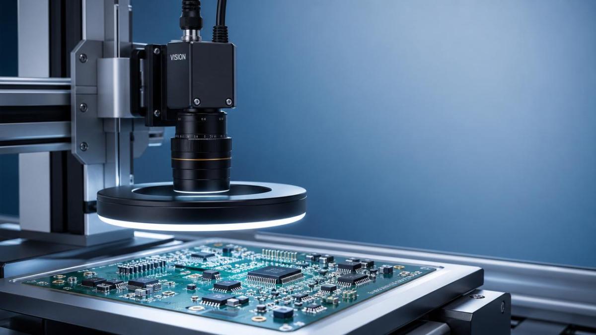
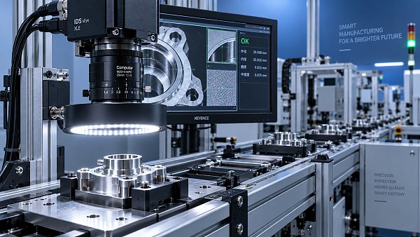
A vision camera for PCB inspection is an industrial imaging device used to capture repeatable, high-contrast images of printed circuit boards for automated defect analysis. In practice, it operates as part of a broader machine vision stack that includes lenses, structured or diffuse illumination, triggering hardware, motion control, and image processing software. The purpose is not simply to “see” the board, but to convert physical assembly conditions into stable pixel data that can be measured against engineering limits.
In PCB environments, the most common inspection tasks include solder joint evaluation, component presence and polarity checks, lead alignment verification, silkscreen reading, barcode identification, pad contamination detection, and post-reflow anomaly screening. The challenge is that solder behaves like a highly reflective surface. Under unsuitable lighting or poor camera positioning, solder glare can saturate bright regions and erase edge detail, making bridges, insufficient wetting, void indicators, or lifted leads harder to classify correctly.
For this reason, a high-performing vision camera for PCB inspection must be evaluated by more than megapixels. Critical factors include sensor dynamic range, pixel size, shutter type, frame stability, signal-to-noise ratio, optical distortion, and compatibility with polarized or angled lighting setups. A technically sound system reduces ambiguity by ensuring that the same defect appears the same way across shifts, batches, and board revisions.
Industry Background and Current Attention Points
Electronics assembly is moving toward finer pitch devices, higher board density, faster takt times, and tighter traceability requirements. These changes are increasing the demand for a vision camera for PCB inspection that can deliver stable results under reflective, high-mix production conditions. The issue is especially visible in SMT lines where solder finish, paste volume variation, and board warpage can alter reflectivity from one panel to the next.
Within this context, solder glare has become a central engineering concern. Excessive reflection can make an acceptable joint appear overexposed, while a true defect may blend into surrounding highlights. This is why data-driven inspection teams increasingly treat lighting design and camera response as measurable process parameters. In line with TSV’s engineering-first view, the value of a vision camera for PCB inspection lies in tolerance control, not in generic claims about image quality.
Why Solder Glare Disrupts Inspection Reliability
Solder glare occurs when direct or partially direct reflections from metallic or semi-metallic joint surfaces enter the lens and overwhelm local contrast. The result is highlight clipping, washed-out boundaries, and unstable grayscale segmentation. This affects both rule-based algorithms and AI-assisted inspection models because both depend on consistent visual features.
Several physical conditions make glare worse:
- Low-angle direct lighting pointed toward the lens axis
- Highly polished or uneven solder surfaces after reflow
- Large height differences between adjacent components
- Insufficient camera dynamic range in mixed bright-dark fields
- Lens flare or poor optical shielding from stray light
When glare is not controlled, three costly outcomes follow. First, false rejects rise because normal joints cross brightness thresholds unexpectedly. Second, escape risk increases because actual bridging or insufficient fillet shape may be hidden under saturated reflections. Third, recipe maintenance becomes unstable, as parameter sets that work on one lot fail on another. A robust vision camera for PCB inspection must therefore support imaging techniques that preserve usable defect features under changing reflective conditions.
Application Value and Business Significance
Selecting the right vision camera for PCB inspection has direct operational consequences across yield, traceability, and process confidence. In electronics production, inspection is not an isolated gate; it is a feedback mechanism linking stencil printing, placement accuracy, reflow behavior, and downstream reliability. Better imaging quality improves defect classification accuracy, which in turn improves root-cause analysis and corrective action speed.
The practical value can be summarized in four areas:
- Lower false call rates: Stable contrast reduces unnecessary manual review and reinspection load.
- Better defect capture: Controlled glare reveals solder geometry, bridging edges, and lead wetting transitions more reliably.
- Higher process repeatability: Consistent images support recipe reuse across lots, lines, and shifts.
- Stronger data trust: When image acquisition is stable, trend data becomes useful for engineering decisions rather than anecdotal troubleshooting.
This aligns with broader hard-tech benchmarking principles. Parameters such as field of view, minimum resolvable feature size, exposure repeatability, and lighting angle should be documented and verified. The best vision camera for PCB inspection is the one that performs predictably under actual board reflectivity, not the one with the most aggressive brochure specification.
Typical PCB Inspection Scenarios and Camera Requirements
Different board types and defect modes require different imaging strategies. A single configuration rarely performs equally well across every product family, especially where solder glare behavior changes with package geometry and surface finish.
For many lines, a monochrome vision camera for PCB inspection provides stronger contrast control than a color camera, especially where grayscale segmentation is critical. Color imaging becomes more useful when distinguishing marking types, residue tones, or mixed material states. The choice should be tied to defect mechanisms, not general preference.
Practical Recommendations for Reducing Solder Glare
A structured approach usually delivers better results than replacing hardware blindly. The following practices are effective when specifying or tuning a vision camera for PCB inspection for reflective solder conditions:
- Match resolution to feature size: Define the smallest defect of interest first, then calculate pixel coverage instead of buying excess resolution without optical justification.
- Use lighting before software compensation: Diffuse dome, dark-field, segmented ring, or polarized setups often solve glare at the source more effectively than post-processing.
- Verify dynamic range under production extremes: Test shiny, dull, and borderline solder joints in one image set to confirm that highlight clipping does not erase defect cues.
- Control mechanical repeatability: Camera angle drift, vibration, and focus variation can reintroduce glare inconsistency even with good components.
- Benchmark with real defect libraries: Qualification should include true production samples, not only ideal reference boards.
- Track false reject and escape metrics together: Reducing one while worsening the other is not a real optimization.
It is also useful to document illumination angle, working distance, aperture, gain, exposure time, and inspection pass/fail thresholds as controlled process parameters. This creates a traceable baseline for future board launches and helps isolate whether a performance shift comes from product change, lighting degradation, or camera drift.
Next-Step Evaluation Path for a Vision Camera for PCB Inspection
A disciplined evaluation path begins with board-level risk mapping. Identify which defect classes are most sensitive to solder glare, which packages create the strongest reflection variance, and what cycle time limits apply. Then compare candidate configurations of sensor, lens, and lighting against the same golden sample and known defect set. This turns camera selection into an engineering comparison instead of a marketing decision.
For a reliable vision camera for PCB inspection, the most important question is simple: can the system repeatedly separate acceptable solder geometry from true defects under real factory conditions? If the answer is supported by measured contrast stability, controlled glare behavior, and reproducible detection results, the inspection platform becomes a trustworthy source of production truth. That is the standard worth pursuing in any data-driven electronics environment.
Search News
Hot Articles
- Carbon Fiber StructuresHow to Specify Aerospace Carbon Fiber Assemblies for Lightweight, Load-Bearing PartsJul 11, 2026
- Machine VisionXiaomi, Alibaba DAMO Academy Drive Open-Source Robotics Model Ecosystem, Lowering Algorithm Development Barriers for Overseas SMEs Adopting Chinese Robotics SolutionsMar 30, 2026
- Cobots & ArmsShanxi 'AI+' Conference Showcases Embodied Intelligence with Multinational Buyer Engagement: Key Industry ImplicationsMar 30, 2026
Popular Tags
Recommended News
 Jul 11, 2026How to Specify Aerospace Carbon Fiber Assemblies for Lightweight, Load-Bearing PartsAerospace carbon fiber assemblies: learn how to specify laminate design, load data, joining methods, and inspection controls for lighter, reliable load-bearing aerospace parts.Elena Rostova (UAV Systems Researcher)
 Mar 30, 2026Xiaomi, Alibaba DAMO Academy Drive Open-Source Robotics Model Ecosystem, Lowering Algorithm Development Barriers for Overseas SMEs Adopting Chinese Robotics SolutionsXiaomi & Alibaba DAMO Academy's open-source robotics models lower algorithm barriers for global SMEs. Boost efficiency in manufacturing, logistics & smart retail with ROS 2 compatible solutions.TSV Data Lab
 Mar 30, 2026Shanxi 'AI+' Conference Showcases Embodied Intelligence with Multinational Buyer Engagement: Key Industry ImplicationsShanxi 'AI+' Conference highlights embodied intelligence with Tesla, Ubtech & Jiantao showcasing multimodal robotics. 40+ global buyers validated tech on-site, creating new B2B channels for industrial automation & AI solutions.Chen Wei (Automation Lead Engineer)
 Mar 30, 2026Zhongguancun Unveils 6G Integrated Sensing-Computing-Intelligence Platform to Empower Embodied Robots for Global Industrial ApplicationsZhongguancun's new 6G platform revolutionizes industrial robotics with <10ms latency, empowering global automotive, logistics & port automation. Discover how this tech boosts China's smart manufacturing exports.TSV Data Lab
 Mar 30, 2026Mech-Mind Tianjin Embodied Intelligence R&D and Production Base Goes Live, Cutting Delivery Time by 20%–30% for Global Customized AMR+Vision SolutionsMech-Mind's Tianjin AMR+Vision production base cuts delivery time by 20%-30% for欧美 & Latin American markets. Discover how this PLd-certified facility accelerates customized robotics solutions for smart manufacturing and logistics.Chen Wei (Automation Lead Engineer)
 Mar 30, 2026Boao Forum Reveals 'Co-evolution of Big and Small Brains' Trend in Humanoid Robots, China's Embodied Intelligence Accelerates Adaptation to Overseas Manufacturing Service ScenariosDiscover how China's humanoid robots, featuring 'Co-evolution of Big and Small Brains,' are revolutionizing global manufacturing. Learn about Embodied Tian Gong 3.0's ISO compliance and overseas deployment at Boao Forum 2026.Chen Wei (Automation Lead Engineer)
 Mar 30, 2026China Railway Industrial Secures Patent for Embodied Robotics in Material Handling, Boosting High-Precision Delivery Capabilities for Overseas Infrastructure and Manufacturing ProjectsChina Railway Industrial's new patent for embodied robotics in material handling boosts high-precision delivery for global infrastructure & manufacturing. Discover how this innovation enhances logistics accuracy in automotive, rail transit & EPC projects.Chen Wei (Automation Lead Engineer)
 Sep 28, 2026Spindle Runout Measurement in Germany: DIN Standards, Methods, and Acceptance LimitsSpindle runout measurement Germany: explore DIN standards, proven methods, acceptance limits, and audit-ready practices for reliable machining quality.Dr. Marcus Vance
 Sep 27, 2026How to Select Wall-Mount Edge Devices for Space-Constrained Factory NetworksWall mount edge devices for space-constrained factories: evaluate workload, thermal design, power resilience, cable access, and network reliability for smarter deployments.TSV Data Lab
 Sep 26, 2026Machining Tolerance Analysis: How to Set Limits That Meet Function and Cost TargetsMachining tolerance analysis: learn how to set functional limits, control tolerance stacks, reduce inspection risk, and balance precision with production cost.Dr. Marcus Vance
 Sep 25, 2026How to Evaluate an Industrial Infrastructure Data Platform for Multi-Site OperationsIndustrial infrastructure data platform evaluation guide for multi-site operations: compare data quality, edge resilience, interoperability, governance, and scalable proof-of-value criteria.Victor Lin (Chief Software Architect)
 Sep 24, 2026How to Select Machine Vision Optics for Accurate Inspection at Different Working DistancesMachine vision optics selection guide for accurate inspection at every working distance. Compare FOV, pixel scale, DOF, distortion, lighting, and telecentric options.TSV Data Lab
 Sep 23, 2026How to Evaluate a Machine Vision System Integrator for High-Speed Inspection LinesChoose a machine vision system integrator with proven expertise in high-speed inspection, reliable reject timing, robust optics, and measurable acceptance criteria.TSV Data Lab
 Sep 28, 2026When is a SCADA API the right choice for connecting plant systems?SCADA API guide: learn when governed plant data integration improves traceability, security, and scalability—without compromising real-time control.Victor Lin (Chief Software Architect)
 Sep 27, 2026How SCADA data integration improves traceability across production linesSCADA data integration connects production-line data to improve traceability, accelerate quality investigations, and strengthen safety decisions.Victor Lin (Chief Software Architect)
 Sep 26, 2026What to define before starting SCADA integration planningSCADA integration planning starts with clear scope, control boundaries, data models, cybersecurity, and testing. Discover the definitions that reduce risk and costly rework.Victor Lin (Chief Software Architect)
 Sep 25, 2026How a smart factory with Industrial IoT reduces production blind spotsDiscover how a smart factory with Industrial IoT turns real-time machine, quality, and workflow data into actionable insights that reduce production blind spots and delivery risks.Victor Lin (Chief Software Architect)
 Sep 24, 2026When does Industrial IoT make smart manufacturing easier to scale?Smart manufacturing Industrial IoT scales when trusted data, interoperable systems, and secure workflows turn connected assets into measurable gains.TSV Data Lab
 Sep 23, 2026What drives ultra-precision machining cost at 1-micron tolerance?Ultra precision machining cost per part at 1 micron tolerance depends on process, material, metrology, and yield. Learn how to compare quotes confidently.Dr. Marcus Vance
 Sep 22, 2026Drone Engine-T550CC Applications: Build the UAV Power System Around the MissionAn application guide for Drone Engine-T550CC integration, covering payload planning, airframe matching, cooling, fuel, vibration, test procedures, documentation, and service preparation.Elena Rostova (UAV Systems Researcher)
 Sep 22, 2026How to Evaluate Industrial Edge Computing Vendors for Factory DeploymentIndustrial edge computing vendor evaluation guide for factories: compare latency, protocol fit, reliability, security, and lifecycle support before deployment.TSV Data Lab
 Sep 21, 2026Drone Payload Integration: Matching Power, Data, and Center of Gravity for Reliable FlightsDrone payload integration made practical: balance power, data, center of gravity, and endurance to build safer, more reliable mission-ready flights.Elena Rostova (UAV Systems Researcher)
 Sep 20, 2026Autonomous Navigation Pricing: Cost Drivers and Budget Benchmarks for AMR ProjectsAutonomous navigation price explained: compare AMR cost drivers, software, sensors, integration, safety, and lifecycle budgets to build a scalable project plan.Chen Wei (Automation Lead Engineer)
 Sep 19, 2026How to Scope Automation Integration Services for Multi-System Factory ProjectsAutomation integration services: learn how to scope multi-system factory projects with clear workflows, interface contracts, safety boundaries, and acceptance criteria.Victor Lin (Chief Software Architect)